(China (Mainland))

Product Summary
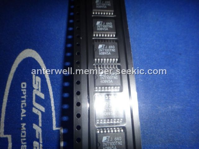
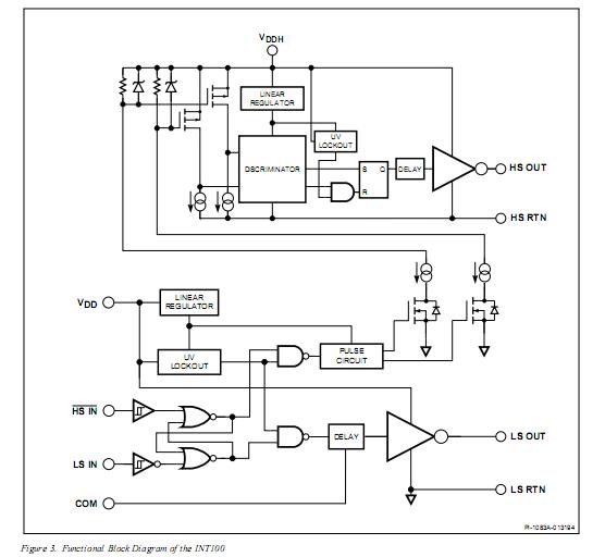
The INT100TNI is a half-bridge driver IC. It provides gate drive for external low-side and high-side MOSFET switches. The INT100TNI also provides a simple, cost-effective interface between low-voltage control logic and high-voltage loads. The INT100TNI is designed to be used with rectified 110 V or 220 V supplies. Both high-side and low-side switches can be controlled independently from ground-referenced 5 V logic inputs.
Parametrics
INT100TNI absolute maximum ratings: (1)VDD Voltage:16.5V; (2)VDDH Voltage:HS RTN + 16.5V; (3)HS RTN:800V - VDDH to -VDDH; (4)HS RTN Slew Rate:10V/ns; (5)Logic Input Voltage:-0.3V to 5.5V; (6)LS OUT Voltage:LS RTN - 0.3V to VDD + 0.3V; (7)HS OUT Voltage:HS RTN - 0.3V to VDDH + 0.3V; (8)Storage Temperature:–65℃ to 125℃; (9)Ambient Temperature:-40℃ to 85℃; (10)Junction Temperature:150℃; (11)Lead Temperature:260℃; (12)Power Dissipation:2.3 W or 1.5 W; (13)Thermal Impedance:55℃/W.
Features
INT100TNI features: (1)5 V CMOS Compatible Control Inputs; (2)Combines logic inputs for low and high-side drives; (3)Schmidt-triggered inputs for noise immunity; (4)Can withstand up to 800 V for direct interface to the HV-referenced high-side switch; (5)Pulsed internal high-voltage level shifters reduce power consumption; (6)Provides 300 mA sink/150 mA source current; (7)Can drive MOSFET gates at up to 15 V; (8)External MOSFET allows flexibility in design for various motor sizes; (9)Simultaneous conduction lockout protection; (10)Undervoltage lockout.
Diagrams
 |
 INT100 |
Other |
|
Data Sheet |
Negotiable |
|
||||