(China (Mainland))

Product Summary
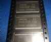
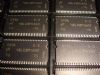
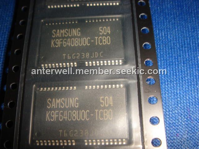
The K9F6408UOC-TCBO is an 8M(8,388,608)x8bit NAND Flash Memory with a spare 256K(262,144)x8bit. The K9F6408UOC-TCBO is offered in 3.3V Vcc. Its NAND cell provides the most cost-effective solution for the solid state mass storage market. A program operation programs the 528-byte page in typical 200μs and an erase operation can be performed in typical 2ms on an 8K-byte block. The K9F6408UOC-TCBO is an optimum solution for large nonvolatile storage applications such as solid state file storage, digital voice recorder, digital still camera and other portable applications requiring non-volatility.
Parametrics
K9F6408UOC-TCBO absolute maximum ratings: (1)Voltage on any pin relative to VSS: VIN/OUT:-0.6 to + 4.6V, VCC:-0.6 to + 4.6V, VccQ:-0.6 to + 4.6V; (2)Temperature Under Bias:-10℃ to + 125℃; (3)Storage Temperature:-65℃ to + 150℃.
Features
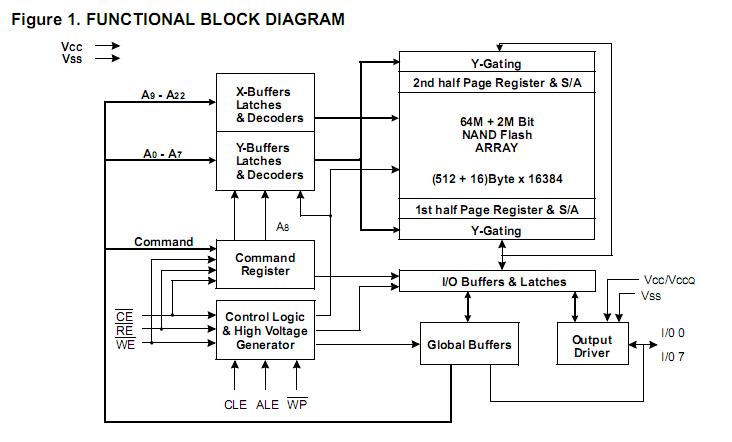
K9F6408UOC-TCBO features: (1)Voltage Supply:1.70 to 1.95V; (2)Organization:Memory Cell Array: (8M + 256K)bit x 8bit, Data Register: (512 + 16)bit x8bit; (3)Automatic Program and Erase: Page Program : (512 + 16)Byte, Block Erase: (8K + 256)Byte; (4)528-Byte Page Read Operation: Random Access : 10μs(Max.), Serial Page Access:50ns; (5)Fast Write Cycle Time: Program Time : 200μs(Typ.), Block Erase Time : 2ms(Typ.); (6)8M x 8 Bit Bit NAND Flash Memory; (7)Command/Address/Data Multiplexed I/O Port; (8)Hardware Data Protection: Program/Erase Lockout During Power Transitions; (9)Reliable CMOS Floating-Gate Technology: Endurance : 100K Program/Erase Cycles, Data Retention : 10 Years; (10)Command Register Operation.
Diagrams
 |
 K9F6408U0M-TIB0 |
Other |
|
Data Sheet |
Negotiable |
|
||||
|
K9F6408U0B-TCB0 |
Other |
|
Data Sheet |
Negotiable |
|
||||
|
K9F6408U0A-TCB0 |
Other |
|
Data Sheet |
Negotiable |
|
||||
|
K9F6408Q0C |
Other |
|
Data Sheet |
Negotiable |
|
||||
|
K9F6408U0M-TCB0 |
Other |
|
Data Sheet |
Negotiable |
|
||||
|
K9F6408U0C-QCB0 |
Other |
|
Data Sheet |
Negotiable |
|
||||